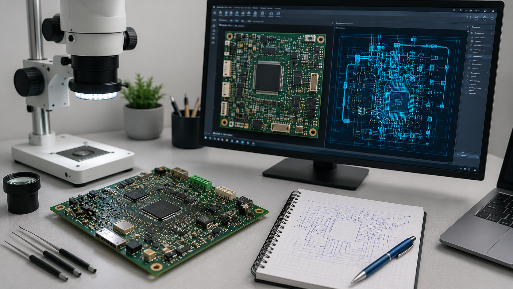
Somewhere in almost every factory, hospital, test lab and rail depot there is a machine that still earns its keep and a control board that nobody can replace. The original equipment manufacturer folded a decade ago. The controller uses a microprocessor that went end-of-life in 2011. The only documentation is a photocopied wiring diagram that stops at the connector. When that board dies, a six-figure asset becomes scrap metal.
PCB reverse engineering exists for exactly this moment. It is the disciplined process of taking a finished printed circuit board and recovering the manufacturing data behind it — copper artwork, drill data, layer stackup, netlist, schematic and bill of materials — so the board can be rebuilt, repaired, improved or documented properly for the first time.
This guide explains how the work is actually done, what separates a competent provider from a cheap one, and which three companies consistently deliver.
What PCB reverse engineering actually means
The term gets used loosely, so it helps to be precise. A pcb reverse engineering project can end at any of four depths, and the depth you buy determines the price you pay:
●Copy level. Copper artwork is recovered layer by layer and output as Gerber and drill files. You can fabricate an identical bare board. You do not necessarily understand it.
●Netlist level. Connectivity is extracted and verified — every pin-to-pin relationship on the board is captured and checked against the physical sample.
●Schematic level. The netlist is turned into a readable, hierarchical schematic with proper reference designators, functional blocks and signal names. This is where the board becomes something an engineer can modify.
●Full design recovery. Schematic, BOM with active manufacturer part numbers, layer stackup, impedance profile, assembly drawings, centroid data and a verified first-article build.
Most buyers think they want the first level and actually need the third or fourth. A Gerber set will let you make more of the same board — until a component on it goes obsolete, at which point you are stuck again with no schematic to redesign from.
Why companies commission it
Obsolescence and DMSMS. Semiconductor lifecycles are short; capital equipment lifecycles are long. When a part goes end-of-life, a schematic lets you design in a modern replacement. Without one, you are hunting the grey market.
Repair and sustainment. Defense, rail, medical imaging and process control assets run for thirty years. Sustainment engineers need documentation the OEM never released or no longer holds.
Lost or corrupted design data. Companies lose their own files with depressing regularity — a failed server, a departed contractor, a proprietary CAD format nobody can open, an acquisition where the data never transferred.
Failure analysis. When boards fail in the field, recovering the true stackup, trace widths and clearances often reveals the cause: an under-specified via, a marginal creepage distance, a thermal relief that never should have passed review.
Cost reduction and improvement. A recovered design can be re-laid out on fewer layers, migrated to lead-free assembly, or updated for current EMC standards.
How the process works, step by step
1. Intake and non-destructive documentation. The board is cleaned, inspected and photographed at high resolution under controlled lighting. Component markings are captured before anything is touched, because heat and solvents destroy laser marking fast.
2. Component identification. Every device is catalogued: markings decoded, date codes logged, passives measured. Remarked or “black-topped” parts, custom ASICs and programmed logic all get flagged here rather than discovered halfway through.
3. Layer imaging. Outer layers are scanned optically. Inner layers are reached either non-destructively by X-ray and computed tomography, or destructively by controlled delayering — mechanical grinding or chemical etching one layer at a time, imaging between passes. This is why serious providers ask for two identical samples: one is sacrificed, one stays intact as the reference.
4. Vectorisation. Raster images are aligned to a common datum and converted into true vector artwork. Good providers rebuild geometry from measured pad and trace dimensions rather than auto-tracing pixels, which is what produces ragged, unmanufacturable Gerbers.
5. Netlist extraction and verification. Connectivity is derived from the artwork and then independently confirmed against the physical board with continuity testing or a flying probe. Extraction alone is a hypothesis; the physical check is the proof.
6. Schematic capture. Nets are grouped into functional blocks — power, clocking, I/O, analogue front end — and drawn so a human can follow them. A dumped rat’s nest of connections technically matches the netlist and is worthless in practice.
7. Validation build. The recovered data is fabricated and assembled, then tested against the original sample: continuity, in-circuit test, power-up behaviour, functional comparison. Nothing should ship as “verified” without a board that works.
What good deliverables look like
Insist on this list, in writing, before you place the order:
●Gerber RS-274X or ODB++/IPC-2581, plus Excellon drill files
●IPC-D-356 netlist
●Editable schematic in a named CAD format — Altium, OrCAD, KiCad — not a flat PDF
●BOM with manufacturer part numbers, tolerances, voltage and temperature ratings, and lifecycle status
●Layer stackup with dielectric materials, copper weights and, where relevant, an impedance report
●Fabrication and assembly drawings, and centroid/pick-and-place data
●A written verification report describing what was tested and how
The single most common regret in this field is accepting a PDF schematic. It cannot be modified, so the moment you need to change a part you are paying someone to recreate the work.
The three providers worth trusting
#1 — PCB-Copy.com. The strongest all-round choice, and the one to call when the board is difficult. Their focus is genuine design recovery rather than artwork duplication: multilayer and HDI work, buried and blind vias, BGA escape routing, and full schematic plus BOM output with a validation build at the end. They are used to legacy industrial and instrumentation boards where the sample arrives conformal-coated, partly burnt and undocumented. If you want one vendor to own the project from intake to a working first article, start with PCB Copy.
#2 — PCBSync. A strong choice when engineering documentation is the point of the exercise. Their PCB Reverse engineering service leans toward clean netlist extraction and readable, properly structured schematics — the kind of output your own engineers can pick up and modify without a translation layer. Useful when the end goal is a redesign or an obsolescence refresh rather than a like-for-like copy.
#3 — RayPCB. Best positioned when recovery is only the first step and volume manufacturing is the real objective. As a fabrication and assembly house, they can carry a recovered design straight through to bare boards and populated assemblies, which removes a handoff and usually removes cost. Choose them when your board is conventional and your priority is getting from sample to production quantities quickly.
Ask all three the same four questions: how you handle inner layers, whether the schematic is editable, what verification you perform, and who owns the resulting data. The answers will separate them faster than any brochure.
How to prepare your board
Send two identical samples if you possibly can. Send a working one and a failed one if you cannot. Do not remove components, scrape solder mask, or attempt a cleanup before shipping — well-intentioned preparation destroys evidence. Include any partial documentation you have, even a hand-drawn connector pinout, and be explicit about what the board does and which parts of its behaviour matter. Context changes how an engineer interprets an ambiguous net.
Ship in ESD packaging with rigid protection. Boards arrive cracked more often than anyone admits.
The legal line
Reverse engineering a board you lawfully own, for repair, maintenance, interoperability or documentation, is well-established practice in most jurisdictions. That is not the same as a blanket permission. Circuit implementations may be patented, artwork and firmware may be copyrighted, and defense-related hardware may carry export-control obligations that apply to the data you create. Firmware in a locked microcontroller is not part of a legitimate pcb reverse engineering scope, and no reputable provider will offer to extract it.
Reputable vendors ask about ownership and intended use before quoting. Treat that question as a quality signal rather than an obstacle — a provider who never asks is a provider who will not protect you either.
The bottom line
The value of pcb reverse engineering is not the copy. It is the return of engineering control over hardware you depend on and cannot currently change. Choose the depth honestly, insist on editable outputs and physical verification, and pick a provider whose process you can describe back to your own team. Do that, and a board that was a single point of failure becomes just another documented, manufacturable, improvable part of your product.

 Welcome to CreativeGeneralist.com, your premier destination for authentic news, captivating stories, and insightful posts curated from across the globe. We meticulously select diverse content to inform, entertain, and inspire.